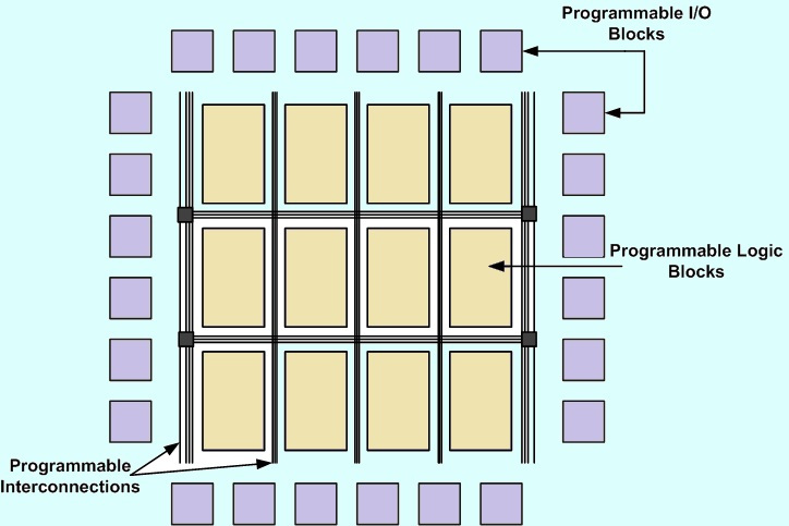

An FPGA has three main elements, Look-Up Tables (LUT), flip-flops, and the routing matrix, that all work together to create a very flexible device.
Look-Up Tables
Look-up tables are how your logic actually gets implemented. A LUT consits of some number of inputs and one output. What makes a LUT powerful is that you can program what the output should be for every single possible input.
A LUT consists of a block of RAM that is indexed by the LUT’s inputs. The output of the LUT is whatever value is in the indexed location in it’s RAM.
As an example let’s look at a 2-input LUT.
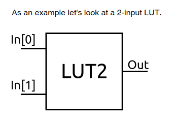
Since the RAM in the LUT can be set to anything, a 2 input LUT can become any logic gate!
For example, if we want to implement an AND gate the contents of the RAM would look like this.
| Address (In[1:0]) | Value (Out) |
|---|---|
| 00 | 0 |
| 01 | 0 |
| 10 | 0 |
| 11 | 1 |
You’re designing a digital circuit more than anything else, basically at one layer of abstraction above the logic gate (AND, OR, NOT) level. At the most basic level, you need to think about how you’re specifying the layout and equations at the level of LUTs (Look-Up Tables) and FFs (Flip-Flops).
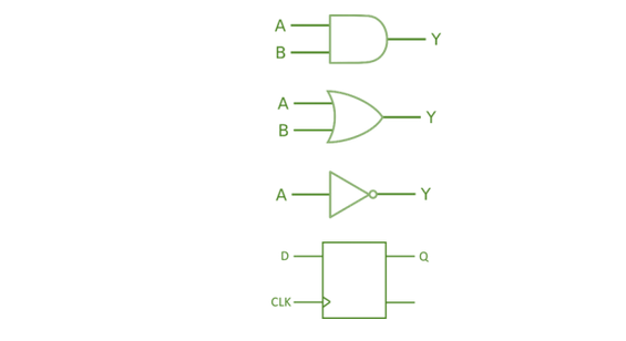
The Logic Blocks, called CLBs (Configurable Logic Blocks) by some FPGA vendors (namely Xilinx), vary in architecture according to the FPGA’s vendor and family. Below is a typical, yet simple, CLB.
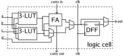
This CLB contains two 3-input LUTs (Look-Up Tables), which in reality are two small 8-bit RAMs, usually used to emulate any 3-input combinational (or combinatorial) function. Combining the two 3-input LUTs with a two-input MUX (multiplexer), we can implement any 4-input combinational function. This CLB also has a full-adder cell (FA), some MUXes and a type-D flip-flop (DFF). So, this CLB can be a part of either combinational or sequential digital complex (with many gates and flip-flops) circuits.
Another important FPGA vendor, the former Altera (now Intel-FPGA, because Intel bought Altera a few months ago), calls Logic Elements (LEs) to their logic blocks. Below is a LE from its Cyclone II family, a block somewhat similar to the CLB from Xilinx (which was shown in the previous picture).
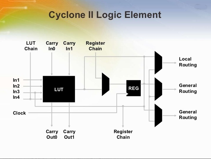
To reconfigure (or “program”) the FPGA, we usually describe the digital circuit we wish to implement in the FPGA using the Verilog or VHDL hardware description languages (HDLs). This description is “compiled” (what is usually called hardware compilation) to a stream of bits which is downloaded, through an FPGA pin, to a register chain inside the FPGA.
This register chain traverses all the programmable registers in the FPGA: LUTs, MUXes and FFDs in the logic blocks, MOSFET switches in the programmable interconnects, and eventually other internal registers (i.e., for instance, registers in the I/O blocks).
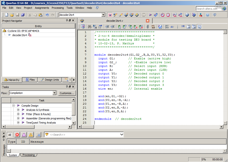
Below is an image of the Quartus II IDE (Integrated Development Environment) from Altera (or Intel-FPGA), where a digital circuit, described as a Verilog module, is shown. It is a simple decoder/demultiplexer, if the comments in the figure are true 🙂
In fact it consists of only five interconnected AND gates.
The IDE from Xilinx has a very similar aspect. Below is an image of the ISE software from Xilinx.
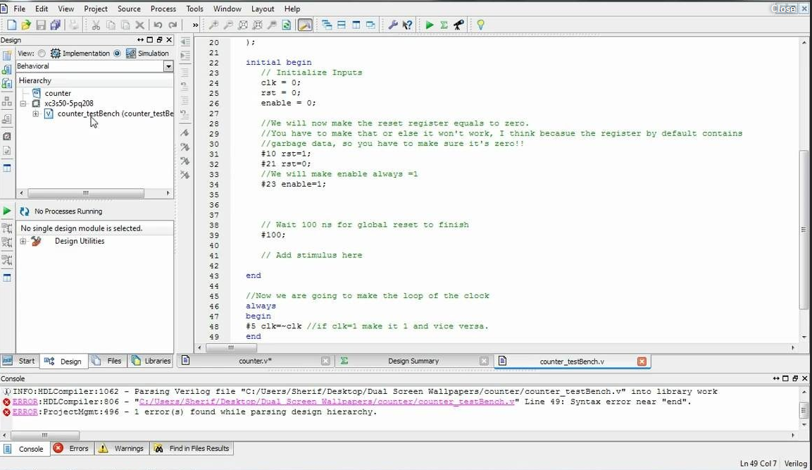
In fact, if you learn to work with one of these tools, it is quite straightforward to extend your skills to the tools from other vendors, given that they are quite similar.
Recall that after you have finished describing your project in one of these design tools, by defining Verilog or VHDL modules (or entities), or even by drawing the circuit schematics, which is also allowed in most of the tools, you compile your design to a bit-file conforming with the FPGA model where you want to deploy your project.
This bit file is then downloaded to the FPGA, and then you can connect other devices and signals to the FPGA (clocks, enables, etc…) and test your design observing its behavior with oscilloscopes and digital signal analyzers.
Programmable Routing
The programmable routing establishes a connection between logic blocks and Input/Output blocks to complete a user-defined design unit.
It consists of multiplexers pass transistors and tri-state buffers. Pass transistors and multiplexers are used in a logic cluster to connect the logic elements.
Programmable I/O
The programmable I/O pads are used to interface the logic blocks and routing architecture to the external components. The I/O pad and the surrounding logic circuit form as an I/O cell.
These cells consume a large portion of the FPGA’s area. And the design of I/O programmable blocks is complex, as there are great differences in the supply voltage and reference voltage.
The selection of standards is important in I/O architecture design. Supporting a large number of standards can increase the silicon chip area required for I/O cells.
With advancement, the basic FPGA Architecture has developed through the addition of more specialized programmable function blocks.
The special functional blocks like ALUs, block RAM, multiplexers, DSP-48, and microprocessors have been added to the FPGA, due to the frequency of the need for such resources for applications.
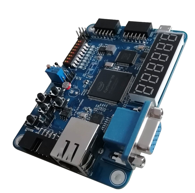
The below snap shows an example of an FPGA Board.

![A fatal error or timeout occurred while processing this directive. [show] [close] A fatal error or timeout occurred while processing this directive. [show] [close]](https://forum.powerhoster.com/wp-content/uploads/2024/10/dberrors-300x168.png)


